|
PAST |
March 26,
2001 |
NEXT |
 |
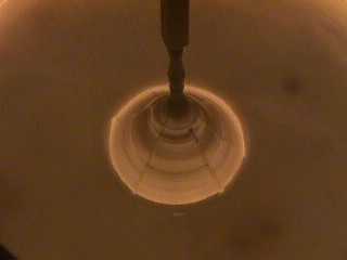
Okay, this isn't really a botanical object here
but I liked the picture.
They do, however, grow these crystal from what they call a
"seed".
This is silicon. That's right the stuff that
microchips are made out of.
All those little mysterious components in your computers, cell phones,
stereos,
TV's, calculators, and almost all other electronic devices,
appliances,
components and accessories.
Silicon is used all over the world and it all
starts from this little
process right here.
They melt the raw silicon down in high
temperature furnaces, 1400 degrees
Celsius to be exact. (That's about 2552 degrees Fahrenheit.)
Silicon is a
natural element on this planet and is quite abundant. Sand is
basically
silicon. However, it takes a considerable amount of resources and
process to
break it down and purify it to be used in standard applications.
Silicon has the properties to be somewhat
conductive (which is why it is
referred to as a "semiconductor") and the resistance
can be controlled by
adding other elements to it to make it more or less conductive,
depending on
the desired process.
After the silicon is melted they drop a small
piece of crystal as you can
see at the top or "stem" of the crystal in the picture.
This small piece is
what they call a seed. This seed is made from a specific
orientation. Crystal
orientation is like the grains in wood and normally grows
radically as an
element freezes from a liquid to a solid state. As they grow it
this
orientation in silicon can be controlled and maintained
throughout the
crystal growth and structure. You can see the small lines, or nodes, on the
surface of
the crystal sides. This is an indication that the crystal is
maintaining the
proper orientation. This orientation is crucial to later
processes in the
manufacture of the integrated circuits.
Once the seed is dipped into the molten
silicon they can turn the
temperature down slightly and freeze the molten silicon to the
seed while
maintaining a specific diameter of what is then referred to as an
ingot.
This ingot is grown to specific lengths and
diameter as per requirements.
Some companies are working with and growing 12" diameter crystals while
others are still working with much smaller diameters.
Once this crystal is grown it can then be sliced
it into very thin wafers,
polished down to a mirrored surface, and then can have circuits printed on them.